- 您现在的位置:买卖IC网 > Sheet目录1902 > AT32UC3C2512C-A2UT (Atmel)IC MCU AVR32 512K FLASH 64TQFP
85
32117DS–AVR-01/12
AT32UC3C
Note:
1. These values are based on simulation and characterization of other AVR microcontrollers manufactured in the same pro-
cess technology. These values are not covered by test limits in production.
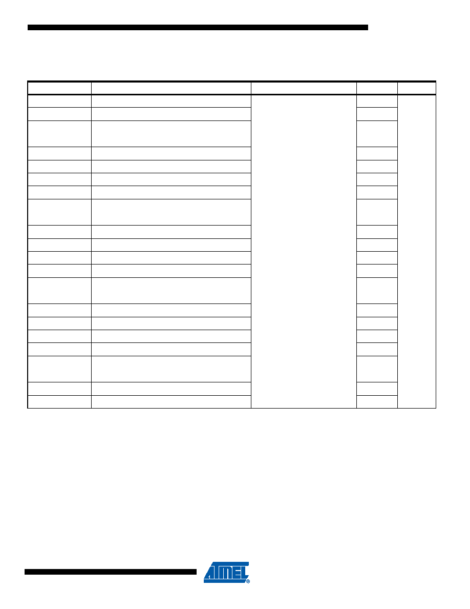
Table 7-58.
SDRAM Signal(1)
Symbol
Parameter
Conditions
Min
Units
SDRAMC1
SDCKE high before SDCK rising edge
VVDD = 3.0V,
drive strength of the pads set to
the highest,
external capacitor = 40pF on
SDRAM pins
except 8 pF on SDCK pins
5.6
ns
SDRAMC
2
SDCKE low after SDCK rising edge
7.3
SDRAMC3
SDCKE low before SDCK rising edge
6.8
SDRAMC4
SDCKE high after SDCK rising edge
8.3
SDRAMC
5
SDCS low before SDCK rising edge
6.1
SDRAMC6
SDCS high after SDCK rising edge
8.4
SDRAMC7
RAS low before SDCK rising edge
7
SDRAMC
8
RAS high after SDCK rising edge
7.7
SDRAMC9
SDA10 change before SDCK rising edge
6.4
SDRAMC10
SDA10 change after SDCK rising edge
7.1
SDRAMC
11
Address change before SDCK rising edge
4.7
SDRAMC12
Address change after SDCK rising edge
4.4
SDRAMC13
Bank change before SDCK rising edge
6.2
SDRAMC
14
Bank change after SDCK rising edge
6.9
SDRAMC15
CAS low before SDCK rising edge
6.6
SDRAMC16
CAS high after SDCK rising edge
7.8
SDRAMC
17
DQM change before SDCK rising edge
6
SDRAMC18
DQM change after SDCK rising edge
6.7
SDRAMC
19
D0-D15 in setup before SDCK rising edge
6.4
SDRAMC
20
D0-D15 in hold after SDCK rising edge
0
SDRAMC23
SDWE low before SDCK rising edge
7
SDRAMC
24
SDWE high after SDCK rising edge
7.4
SDRAMC
25
D0-D15 Out valid before SDCK rising edge
5.2
SDRAMC26
D0-D15 Out valid after SDCK rising edge
5.6
发布紧急采购,3分钟左右您将得到回复。
相关PDF资料
AT32UC3C2512C-A2ZT
IC MCU 32BIT 512KB FLASH 64TQFP
AT32UC3L016-D3HR
MCU AVR32 16K FLASH 48TTLGA
AT42QT5480-CU QS444
IC SENSOR DUAL TOUCH 49-BGA
AT6010H-4QI
IC FPGA 4NS 240PQFP
AT80C31X2-SLRUM
MCU ROMLESS 31X2 5V 44-PLCC
AT80C51RD2-SLRUM
IC MCU 80C51 HI PERFORM 44PLCC
AT85C51SND3B1-RTTUL
IC DECODER/ENCODER DGTL 100-LQFP
AT87251G2D-RLTUM
IC MCU 8/16BIT 32K OTP 44-VQFP
相关代理商/技术参数
AT32UC3C2512C-A2ZR
功能描述:32位微控制器 - MCU 512KB FL,-40/125oC AUTO
RoHS:否 制造商:Texas Instruments 核心:C28x 处理器系列:TMS320F28x 数据总线宽度:32 bit 最大时钟频率:90 MHz 程序存储器大小:64 KB 数据 RAM 大小:26 KB 片上 ADC:Yes 工作电源电压:2.97 V to 3.63 V 工作温度范围:- 40 C to + 105 C 封装 / 箱体:LQFP-80 安装风格:SMD/SMT
AT32UC3C2512C-A2ZT
功能描述:32位微控制器 - MCU 512KB FL,-40/125oC AUTO
RoHS:否 制造商:Texas Instruments 核心:C28x 处理器系列:TMS320F28x 数据总线宽度:32 bit 最大时钟频率:90 MHz 程序存储器大小:64 KB 数据 RAM 大小:26 KB 片上 ADC:Yes 工作电源电压:2.97 V to 3.63 V 工作温度范围:- 40 C to + 105 C 封装 / 箱体:LQFP-80 安装风格:SMD/SMT
AT32UC3C2512C-Z2UR
制造商:Atmel Corporation 功能描述:MCU 32-bit AT32 AVR RISC 512KB Flash 3.3V/5V 64-Pin QFN EP T/R 制造商:Atmel Corporation 功能描述:512KB FLASH 64QFN(-40?C TO 85?C) T&R - Tape and Reel 制造商:Atmel Corporation 功能描述:IC MCU 32BIT 512KB FLASH 64QFN 制造商:Atmel Corporation 功能描述:32-bit Microcontrollers - MCU 512KB Flash 64QFN (-40oC to 85oC) 制造商:Atmel Corporation 功能描述:512KB Flash 64QFN(-40C to 85C) T&R
AT32UC3C2512C-Z2UT
制造商:Atmel Corporation 功能描述:512KFLASH AUTO - Trays
AT32UC3C2512C-Z2ZES
制造商:Atmel Corporation 功能描述:512KFLASH UC3C AUTO - QFN64 ENG SAMPLE - Bulk
AT32UC3C2512C-Z2ZR
功能描述:32位微控制器 - MCU 512KB FL,-40/125oC AUTO
RoHS:否 制造商:Texas Instruments 核心:C28x 处理器系列:TMS320F28x 数据总线宽度:32 bit 最大时钟频率:90 MHz 程序存储器大小:64 KB 数据 RAM 大小:26 KB 片上 ADC:Yes 工作电源电压:2.97 V to 3.63 V 工作温度范围:- 40 C to + 105 C 封装 / 箱体:LQFP-80 安装风格:SMD/SMT
AT32UC3C2512C-Z2ZT
功能描述:32位微控制器 - MCU 512KB FL,-40/125oC AUTO
RoHS:否 制造商:Texas Instruments 核心:C28x 处理器系列:TMS320F28x 数据总线宽度:32 bit 最大时钟频率:90 MHz 程序存储器大小:64 KB 数据 RAM 大小:26 KB 片上 ADC:Yes 工作电源电压:2.97 V to 3.63 V 工作温度范围:- 40 C to + 105 C 封装 / 箱体:LQFP-80 安装风格:SMD/SMT
AT32UC3C264C-A2UR
功能描述:32位微控制器 - MCU UC3C 64K FLASH 16K SRAM
RoHS:否 制造商:Texas Instruments 核心:C28x 处理器系列:TMS320F28x 数据总线宽度:32 bit 最大时钟频率:90 MHz 程序存储器大小:64 KB 数据 RAM 大小:26 KB 片上 ADC:Yes 工作电源电压:2.97 V to 3.63 V 工作温度范围:- 40 C to + 105 C 封装 / 箱体:LQFP-80 安装风格:SMD/SMT